Semiconductor Plant Design
Overview
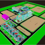
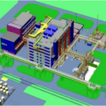
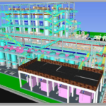
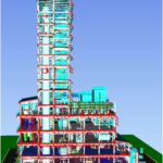
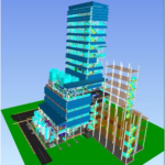
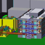
Designing a semiconductor plant (also called a fab or foundry) is an incredibly complex engineering challenge that involves multiple disciplines, including civil, mechanical, electrical, and chemical engineering, as well as cleanroom design, process engineering, and automation.
Key Aspects of Semiconductor Plant Design Engineering
- Location Considerations: Proximity to utilities, stable seismic zones, access to skilled workforce, government incentives
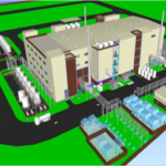
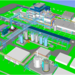
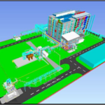
- Utilities & Infrastructure: Requires massive amounts of electricity, water, and gas, with advanced waste treatment and recycling systems.
- Supply Chain & Logistics: Efficient transportation and storage for chemicals, gases, wafers, and finished chips.
- Cleanroom Classification: Semiconductor fabs operate at ISO 4 to ISO 1 (with ISO 1 being the cleanest).
- Air Handling & Filtration: High-efficiency particulate air (HEPA/ULPA) filtration ensures an ultra-clean environment.
- Temperature & Humidity Control: Precise control is critical to prevent contamination and defects.
- Lithography, Etching, Deposition, CMP, Ion Implantation, etc.: Each process requires specific equipment and environmental conditions.
- Workflow Optimization: Efficient movement of wafers through multiple process stages.
- Automation & Robotics: Most fabs use Automated Material Handling Systems (AMHS) with robotic wafer transport.
- Ultra-Pure Water (UPW) Systems: Semiconductor fabs require millions of gallons per day of ultrapure water.
- HVAC & Exhaust Systems: Prevent contamination and handle toxic chemical exhaust safely.
- Power Supply & Backup: Semiconductor plants need uninterruptible power with redundancy.
- Specialty Gases & Chemicals: Including silane, ammonia, hydrogen, and fluorine-based etchants.
- Gas Detection & Safety Systems: Continuous monitoring to prevent leaks and accidents.
- Environmental Regulations: Stringent controls on emissions, wastewater, and hazardous materials.
- Worker Safety & PPE: Cleanroom suits, chemical handling procedures, and emergency response planning.
- AI & Machine Learning: Used for defect detection, process optimization, and predictive maintenance.
- IoT & Digital Twins: Real-time monitoring and modeling of fab operations.